Year
Month
(Peer-Reviewed) Large-scale and high-quality III-nitride membranes through microcavity-assisted crack propagation by engineering tensile-stressed Ni layers
Jung-Hong Min ¹, Kwangjae Lee ², Tae-Hoon Chung ³, Jung-Wook Min ¹, Kuang-Hui Li ¹, Chun Hong Kang ¹, Hoe-Min Kwak ⁴, Tae-Hyeon Kim ⁵, Youyou Yuan ⁶, Kyoung-Kook Kim ⁵, Dong-Seon Lee ⁴, Tien Khee Ng ¹, Boon S. Ooi ¹
¹ Photonics Laboratory, Computer, Electrical and Mathematical Sciences and Engineering Division (CEMSE), King Abdullah University of Science and Technology (KAUST), Thuwal 23955-6900, Saudi Arabia
² Department of Electrical Engineering, Stanford University, Stanford, CA 94305, USA
³ Light Source Research Division, Korea Photonics Technology Institute (KOPTI), Gwangju 61007, Republic of Korea
⁴ School of Electrical Engineering and Computer Science, Gwangju Institute of Science and Technology, Gwangju 61005, Republic of Korea
⁵ Department of Advanced Convergence Technology, Research Institute of Advanced Convergence Technology, Korea Polytechnic University, 237 Sangidaehak-ro, Siheung-si 15073, Republic of Korea
⁶ King Abdullah University of Science and Technology (KAUST), Thuwal 23955-6900, Saudi Arabia
Opto-Electronic Science, 2022-10-28
Abstract

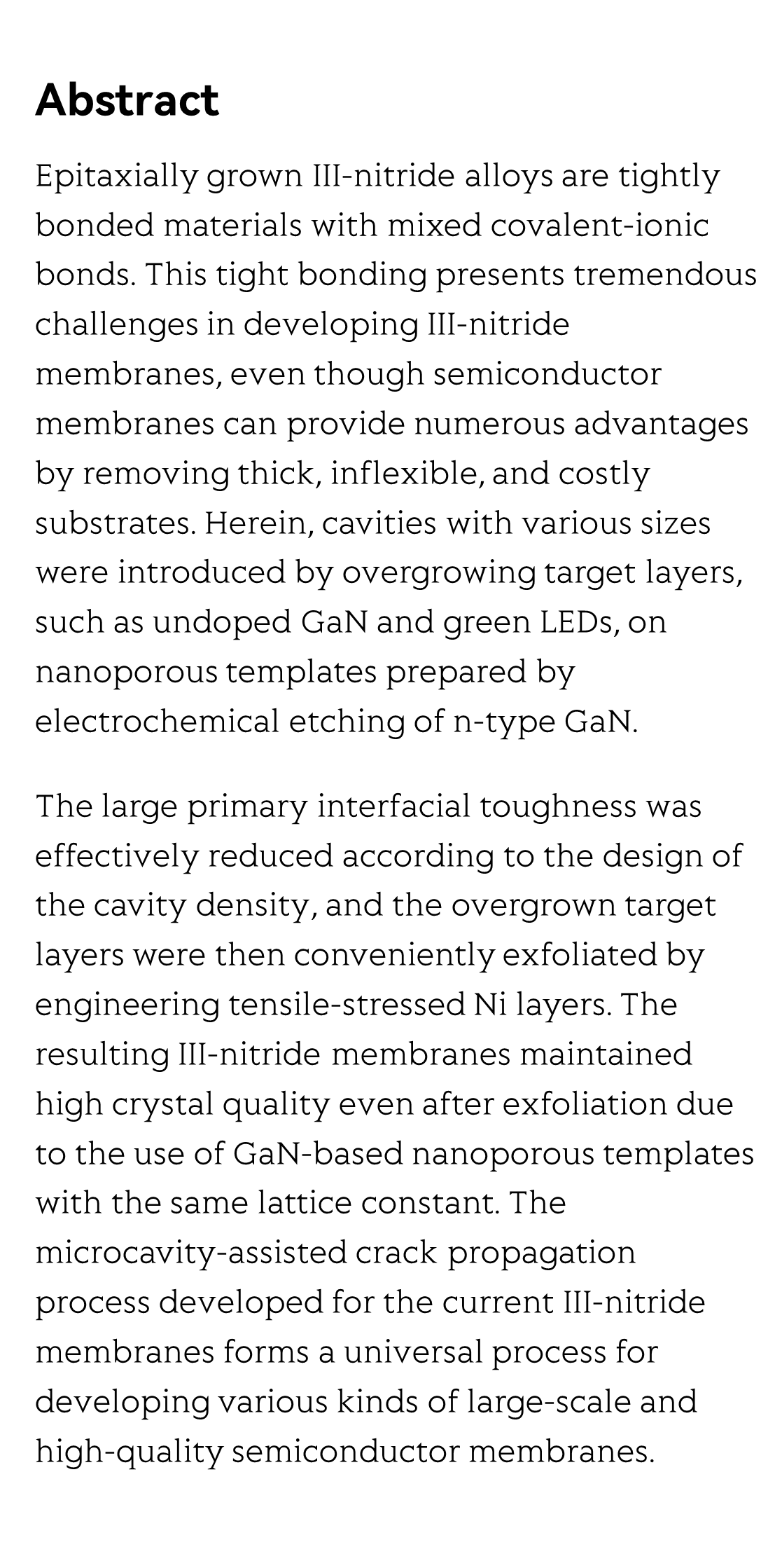
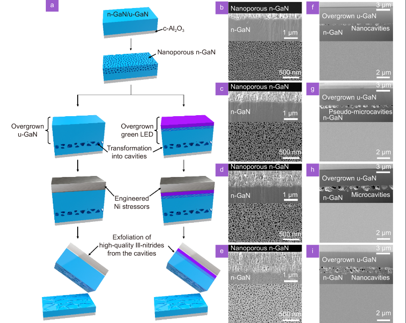
Epitaxially grown III-nitride alloys are tightly bonded materials with mixed covalent-ionic bonds. This tight bonding presents tremendous challenges in developing III-nitride membranes, even though semiconductor membranes can provide numerous advantages by removing thick, inflexible, and costly substrates. Herein, cavities with various sizes were introduced by overgrowing target layers, such as undoped GaN and green LEDs, on nanoporous templates prepared by electrochemical etching of n-type GaN.

The large primary interfacial toughness was effectively reduced according to the design of the cavity density, and the overgrown target layers were then conveniently exfoliated by engineering tensile-stressed Ni layers. The resulting III-nitride membranes maintained high crystal quality even after exfoliation due to the use of GaN-based nanoporous templates with the same lattice constant. The microcavity-assisted crack propagation process developed for the current III-nitride membranes forms a universal process for developing various kinds of large-scale and high-quality semiconductor membranes.
Large-scale and high-quality III-nitride membranes through microcavity-assisted crack propagation by engineering tensile-stressed Ni layers_1
Large-scale and high-quality III-nitride membranes through microcavity-assisted crack propagation by engineering tensile-stressed Ni layers_2
Large-scale and high-quality III-nitride membranes through microcavity-assisted crack propagation by engineering tensile-stressed Ni layers_3
  • Robust measurement of orbital angular momentum of a partially coherent vortex beam under amplitude and phase perturbations
  • Zhao Zhang, Gaoyuan Li, Yonglei Liu, Haiyun Wang, Bernhard J. Hoenders, Chunhao Liang, Yangjian Cai, Jun Zeng
  • Opto-Electronic Science
  • 2024-01-31
  • Deblurring, artifact-free optical coherence tomography with deconvolution-random phase modulation
  • Xin Ge, Si Chen, Kan Lin, Guangming Ni, En Bo, Lulu Wang, Linbo Liu
  • Opto-Electronic Science
  • 2024-01-31
  • Dynamic interactive bitwise meta-holography with ultra-high computational and display frame rates
  • Yuncheng Liu, Ke Xu, Xuhao Fan, Xinger Wang, Xuan Yu, Wei Xiong, Hui Gao
  • Opto-Electronic Advances
  • 2024-01-25
  • Multi-dimensional multiplexing optical secret sharing framework with cascaded liquid crystal holograms
  • Keyao Li, Yiming Wang, Dapu Pi, Baoli Li, Haitao Luan, Xinyuan Fang, Peng Chen, Yanqing Lu, Min Gu
  • Opto-Electronic Advances
  • 2024-01-25
  • Physics-informed deep learning for fringe pattern analysis
  • Wei Yin, Yuxuan Che, Xinsheng Li, Mingyu Li, Yan Hu, Shijie Feng, Edmund Y. Lam, Qian Chen, Chao Zuo
  • Opto-Electronic Advances
  • 2024-01-25
  • Advancing computer-generated holographic display thanks to diffraction model-driven deep nets
  • Vittorio Bianco, Pietro Ferraro
  • Opto-Electronic Advances
  • 2024-01-16
  • Inverse design for material anisotropy and its application for a compact X-cut TFLN on-chip wavelength demultiplexer
  • Jiangbo Lyu, Tao Zhu, Yan Zhou, Zhenmin Chen, Yazhi Pi, Zhengtong Liu, Xiaochuan Xu, Ke Xu, Xu Ma, Lei Wang, Zizheng Cao, Shaohua Yu
  • Opto-Electronic Science
  • 2024-01-09
  • Improved spatiotemporal resolution of anti-scattering super-resolution label-free microscopy via synthetic wave 3D metalens imaging
  • Yuting Xiao, Lianwei Chen, Mingbo Pu, Mingfeng Xu, Qi Zhang, Yinghui Guo, Tianqu Chen, Xiangang Luo
  • Opto-Electronic Science
  • 2024-01-05
  • Wide-spectrum optical synthetic aperture imaging via spatial intensity interferometry
  • Chunyan Chu, Zhentao Liu, Mingliang Chen, Xuehui Shao, Guohai Situ, Yuejin Zhao, Shensheng Han
  • Opto-Electronic Advances
  • 2023-3-10
  • Flat soliton microcomb source
  • Xinyu Wang, Xuke Qiu, Mulong Liu, Feng Liu, Mengmeng Li, Linpei Xue, Bohan Chen, Mingran Zhang, Peng Xie
  • Opto-Electronic Science
  • 2023-12-29
  • Smart palm-size optofluidic hematology analyzer for automated imaging-based leukocyte concentration detection
  • Deer Su, Xiangyu Li, Weida Gao, Qiuhua Wei, Haoyu Li, Changliang Guo, Weisong Zhao
  • Opto-Electronic Science
  • 2023-12-28


  • Carnivorous plants inspired shape-morphing slippery surfaces                                Spatiotemporal Fourier transform with femtosecond pulses for on-chip devices
    About
    |
    Contact
    |
    Copyright © PubCard