(Peer-Reviewed) On-chip light control of semiconductor optoelectronic devices using integrated metasurfaces
Cheng-Long Zheng 郑程龙 ¹, Pei-Nan Ni 倪佩楠 ¹, Yi-Yang Xie 解意洋 ², Patrice Genevet ³
¹ Henan Key Laboratory of Diamond Optoelectronic Materials and Devices, Key Laboratory of Materials Physics, Ministry of Education, School of Physics, Zhengzhou University, Zhengzhou 450052, China
中国 郑州 郑州大学物理学院 材料物理教育部重点实验室 河南省金刚石光电材料与器件重点实验室
² Key Laboratory of Optoelectronics Technology, Beijing University of Technology, Ministry of Education, Beijing 100124, China
中国 北京 北京工业大学光电子技术教育部重点实验室
³ Colorado School of Mines, 1523 Illinois St., Golden, CO 80401, USA
Opto-Electronic Advances
, 2025-01-07
Abstract
Semiconductor optoelectronics devices, capable of converting electrical power into light or conversely light into electrical power in a compact and highly efficient manner represent one of the most advanced technologies ever developed, which has profoundly reshaped the modern life with a wide range of applications. In recent decades, semiconductor technology has rapidly evolved from first-generation narrow bandgap materials (Si, Ge) to the latest fourth-generation ultra-wide bandgap semiconductor (GaO, diamond, AlN) with enhanced performance to meet growing demands.
Additionally, merging semiconductor devices with other techniques, such as computer assisted design, state-of-the-art micro/nano fabrications, novel epitaxial growth, have significantly accelerated the development of semiconductor optoelectronics devices. Among them, integrating metasurfaces with semiconductor optoelectronic devices have opened new frontiers for on-chip control of their electromagnetic response, providing access to previously inaccessible degrees of freedom.
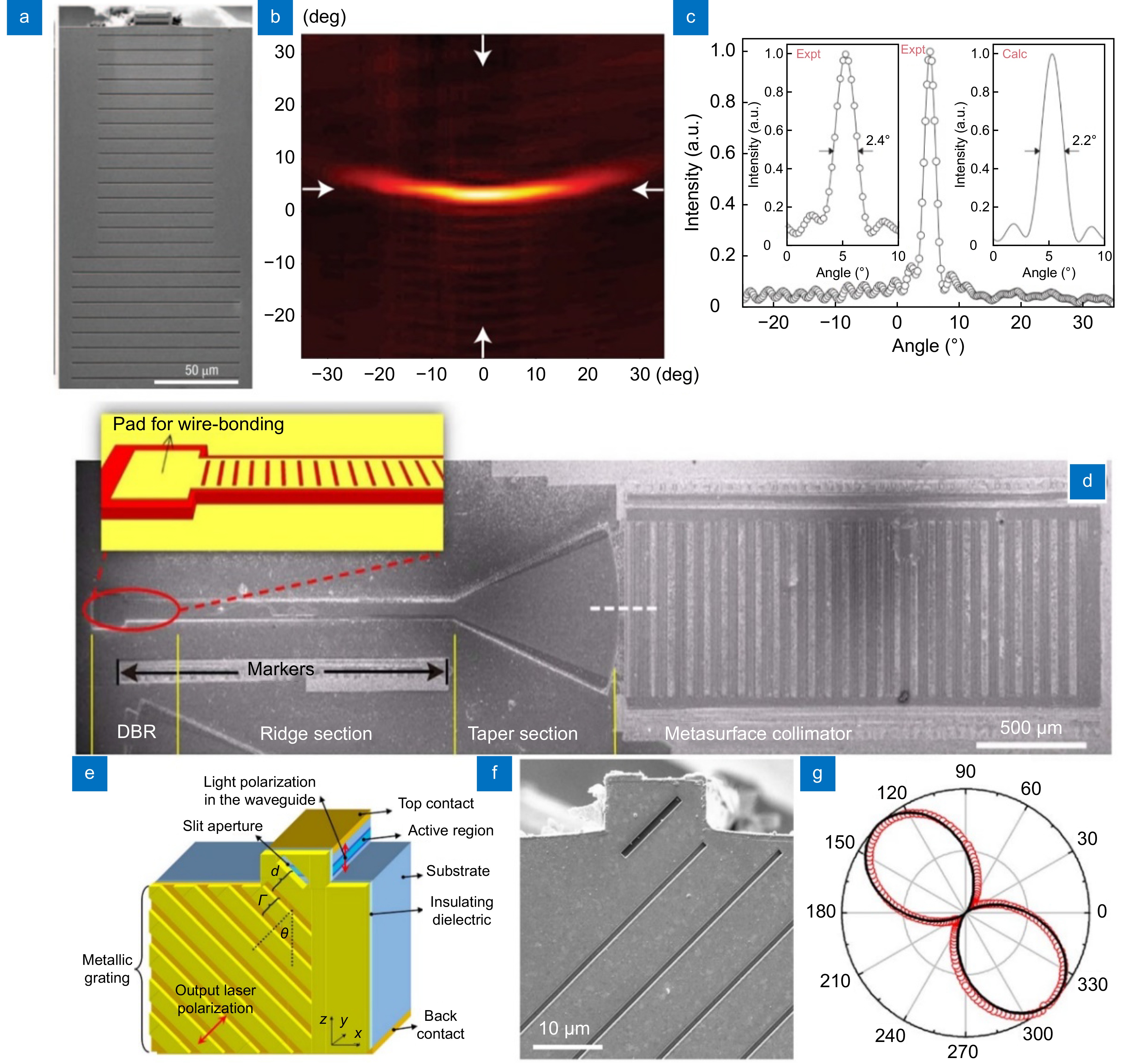
We review the recent advances in on-chip control of a variety of semiconductor optoelectronic devices using integrated metasurfaces, including semiconductor lasers, semiconductor light emitting devices, semiconductor photodetectors, and low dimensional semiconductors. The integration of metasurfaces with semiconductors offers wafer-level ultracompact solutions for manipulating the functionalities of semiconductor devices, while also providing a practical platform for implementing cutting-edge metasurface technology in real-world applications.
Integrated metasurface-freeform system enabled multi-focal planes augmented reality display
Shifei Zhang, Lina Gao, Yidan Zhao, Yongdong Wang, Bo Wang, Junjie Li, Jiaxi Duan, Dewen Cheng, Cheng-Wei Qiu, Yongtian Wang, Tong Yang, Lingling Huang
Opto-Electronic Science
2026-01-23
