(Peer-Reviewed) High performance integrated photonic circuit based on inverse design method
Huixin Qi 齐慧欣 ¹, Zhuochen Du 杜卓晨 ¹, Xiaoyong Hu 胡小永 ¹ ² ³, Jiayu Yang 杨佳宇 ¹, SaiSai Chu 褚赛赛 ¹, Qihuang Gong 龚旗煌 ¹ ² ³
¹ State Key Laboratory for Mesoscopic Physics & Department of Physics, Collaborative Innovation Center of Quantum Matter & Frontiers Science Center for Nano-optoelectronics, Beijing Academy of Quantum Information Sciences, Peking University, Beijing 100871, China
中国 北京 北京大学 人工微结构和介观物理国家重点实验室 量子物质科学协同创新中心 纳光电子前沿科学中心
² Peking University Yangtze Delta Institute of Optoelectronics, Nantong 226010, China
中国 南通 北京大学 长三角光电科学研究院
³ Collaborative Innovation Center of Extreme Optics, Shanxi University, Taiyuan 030006, China
中国 太原 山西省极端光学协同创新中心
Opto-Electronic Advances, 2022-06-01
Abstract
The basic indexes of all-optical integrated photonic circuits include high-density integration, ultrafast response and ultra-low energy consumption. Traditional methods mainly adopt conventional micro/nano-structures. The overall size of the circuit is large, usually reaches hundreds of microns. Besides, it is difficult to balance the ultrafast response and ultra-low energy consumption problem, and the crosstalk between two traditional devices is difficult to overcome.
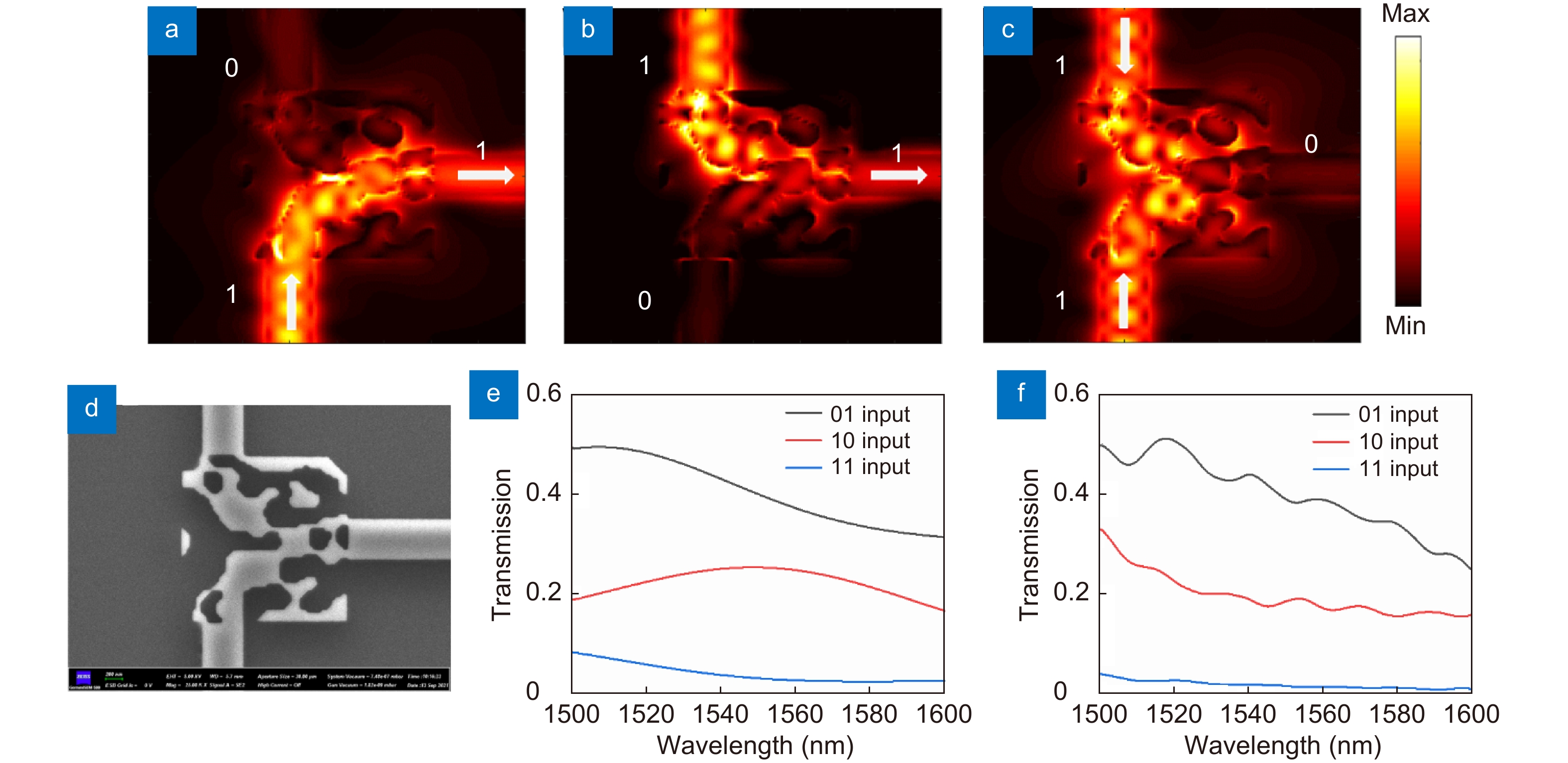
Here, we propose and experimentally demonstrate an approach based on inverse design method to realize a high-density, ultrafast and ultra-low energy consumption integrated photonic circuit with two all-optical switches controlling the input states of an all-optical XOR logic gate. The feature size of the whole circuit is only 2.5 μm × 7 μm, and that of a single device is 2 μm × 2 μm. The distance between two adjacent devices is as small as 1.5 μm, within wavelength magnitude scale. Theoretical response time of the circuit is 150 fs, and the threshold energy is within 10 fJ/bit.
We have also considered the crosstalk problem. The circuit also realizes a function of identifying two-digit logic signal results. Our work provides a new idea for the design of ultrafast, ultra-low energy consumption all-optical devices and the implementation of high-density photonic integrated circuits.
Ultrafast all-optical modulation of wide-bandwidth pulses enabled by silicon-metasurfaces
Kaloyan Georgiev, Khosro Zangeneh Kamali, Anton A. Trifonov, Giulia Crotti, Lyuben Petrov, Stefan Georgiev, Hristo Iliev, Lei Xu, Unai Arregui Leon, Mohsen Rahmani, Giuseppe Della Valle, Ivan Buchvarov, Dragomir Neshev
Opto-Electronic Advances
2026-09-15
Physics-informed neural fields enable blind aberration correction for partially coherent quantitative phase imaging
Shun Zhou, Xingyu Huang, Linpeng Lu, Habib Ullah, Kaiyu Du, Maciej Trusiak, Malgorzata Kujawinska, Yuzhen Zhang, Yao Fan, Qian Chen, Qinrong Zhang, Chao Zuo
Opto-Electronic Science
2026-08-26
Heterogeneously integrated micro-ring with SnS₂ for dual-functional optical modulation and photodetection
Jinyi Du, Lidan Lu, Xu Zhang, Bofei Zhu, Wenbo Bo, Yingjie Xu, Guang Chen, Yanlin He, Guanghui Ren, Xiaoping Lou, Zheng You, Lianqing Zhu
Opto-Electronic Advances
2026-08-25
Hardware-aware lightweight photonic spiking neural network for pattern classification
Shuiying Xiang, Yahui Zhang, Shangxuan Shi, Haowen Zhao, Dianzhuang Zheng, Xingxing Guo, Yanan Han, Ye Tian, Liyue Zhang, Yuechun Shi, Yue Hao
Opto-Electronic Advances
2026-08-25
PhyspeNet: An empirical physics-aware network for adaptive speckle reconstructive spectrometry
Junrui Liang, Min Jiang, Jun Li, Zhongming Huang, Junhong He, Yanting Guo, Yanzhao Ke, Jun Ye, Jiangming Xu, Jinyong Leng, Pu Zhou
Opto-Electronic Advances
2026-08-25
A 36 × 240 Gbps hybrid mode/wavelength division multiplexing transmitter using lithium niobate on insulator
Mingyu Zhu, Weihan Wang, Ruitao Ma, Aoyun Gao, Chun Gao, Zexu Wang, Fei Huang, Zhenyuan Bao, Dajian Liu, Jiaxuan Gan, Zejie Yu, Huan Li, Weike Zhao, Daoxin Dai
Opto-Electronic Advances
2026-08-25