(Peer-Reviewed) Direct growth of hexagonal boron nitride films on dielectric sapphire substrates by pulsed laser deposition for optoelectronic applications
Gaokai Wang 王高凯 ¹ ², Jingren Chen 陈镜壬 ¹ ², Junhua Meng 孟军华 ³, Zhigang Yin 尹志岗 ¹ ², Ji Jiang 江季 ¹ ², Yan Tian 田琰 ¹ ², Jingzhen Li 李景祯 ¹ ², Jinliang Wu 吴金良 ¹ ², Peng Jin 金鹏 ¹ ², Xingwang Zhang 张兴旺 ¹ ²
¹ Key Lab of Semiconductor Materials Science, Institute of Semiconductors, Chinese Academy of Sciences, Beijing, 100083, P. R. China
中国 北京 中国科学院半导体研究所 半导体材料科学重点实验室
² Center of Materials Science and Optoelectronics Engineering, University of Chinese Academy of Sciences, Beijing 100049, P. R. China
中国 北京 中国科学院大学材料科学与光电子工程中心
³ Faculty of Science, Beijing University of Technology, Beijing, 100124, China
中国 北京 北京工业大学理学部
Abstract
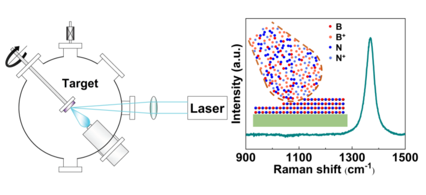
Recently, hexagonal boron nitride (h-BN), an ultra-wide bandgap semiconductor, has attracted considerable attention owing to its excellent properties. In thin films grown on metal catalysts, contamination and damage induced by a transfer process cannot be avoided. Therefore, synthesizing h-BN films on non-catalytic dielectric substrates is desirable for electronic applications.
In this study, we demonstrate the direct growth of high-quality h-BN films with a controllable thickness on sapphire substrates by using the pulsed laser deposition (PLD) technique. The effects of the deposition conditions and laser parameters on the growth of the h-BN films are systematically investigated by evaluating their characteristic Raman peaks. Among the various growth parameters studied, the substrate temperature has the greatest influence on the crystalline quality of the h-BN films, and the optimal pressure varies depending on the target-substrate distance.
The h-BN film grown under optimal conditions exhibits a narrow Raman line width of ∼30 cm⁻¹, indicating a high crystalline quality. The photodetectors fabricated from the PLD-grown h-BN films exhibit superior deep-ultraviolet detection performance with a large on/off ratio of >10⁴, high photoresponsivity, and a sharp cut-off wavelength of 220 nm. This study presents the possibility of producing high-quality h-BN films by applying PLD on dielectric substrates for optoelectronic applications.
Integrated metasurface-freeform system enabled multi-focal planes augmented reality display
Shifei Zhang, Lina Gao, Yidan Zhao, Yongdong Wang, Bo Wang, Junjie Li, Jiaxi Duan, Dewen Cheng, Cheng-Wei Qiu, Yongtian Wang, Tong Yang, Lingling Huang
Opto-Electronic Science
2026-01-23
